48V 遷移之路上的 12 項技術挑戰
為幫助您為遷移到 48V 做好更充分的準備,以下梳理了 12 項需要重點關注的挑戰
要直觀地說明電源時序的重要性,可以設想在一個大型工業系統中,如果其電機和執行器先於控制電子設備通電會發生什麼情况。 顯然,必須通過精心設計的電源啟動順序來徹底消除此類不可預測且危險的隱患。 同樣,關機順序也至關重要。
錯誤的電源時序不僅會在半導體器件層面,還會在系統層面引發問題。 例如,這些問題可能導致 CMOS 器件出現意外的反向偏置,從而損壞或摧毀該器件,或將其鎖定在只能通過重啓電源才能解除的導通狀態。 儘管阻塞二極體可以防止閂鎖效應,但會限制可用類比輸入電壓的範圍,因此採用電源電壓啟動時序是首選解決方案。 此外, DSP、 微處理器等多電壓器件通常要求先提供 I/O 電壓再施加內核電壓。 英特爾處理器晶片檔案中通常會明確說明必須遵循的啟動與關斷順序。 同樣,CPU 晶片必須在系統圖形 IC 之前上電,以防止向圖形顯示器輸出失控訊號。
典型的電源時序方法有兩種:一種基於電源,另一種基於邏輯。
“電源”解決方案利用某一電源軌的電壓上升訊號,向 N 溝道 MOSFET 發送一個適當延遲的觸發訊號,從而控制第二個電源軌的供電。 “邏輯”解決方案則基於電源模組器件(power train device)的使能(Enable)引脚或其他邏輯引脚進行控制,而非直接控制其供電電源。 利用電源組件內部集成的邏輯可實現成本更低、結構更緊湊且更簡潔的解決方案,但在要求更高的應用中,MOSFET 能提供更精確的導通時間控制。
下圖 1 展示了一個採用 N 溝道 MOSFET 和比較器的基礎 MOSFET 時序電路。 VREF 用於設定 VCC2 的切換閾值,VCC2 將在 VCC1 啟動後經過 RC 網路設定的延遲時間才啟動。 MOSFET 驅動器內寘一個電荷泵,確保 VGS 比 VCC2 高出數伏,從而完全增强 MOSFET 切換。 該電路也確保 VCC2 會隨 VCC1 關閉而關斷,但由於 RC 網路的存在,VCC2 的關斷會滯後於 VCC1。 此外,如果 VCC1 無法用作參攷電壓,可能會出現其他問題。
圖 1:採用 RC 網路、比較器和 MOSFET 驅動器的電源時序
圖 1:採用 RC 網路、比較器和 MOSFET 驅動器的電源時序
目前已有集成度更高、更簡便的解決方案,如圖 2 所示的示例。
圖 2:採用 MAX6819 的電源時序
圖 2:採用 MAX6819 的電源時序
該時序器確保 MOSFET 始終獲得所需的最小 VGS 增强電壓,從而最大限度地减少 MOSFET 的損耗,並確保較低的漏源阻抗(RDS(ON))。 MAX6819 預設了 200ms 的出廠固定延遲時間,該延遲發生在主電壓超過設定閾值之後、啟用電荷泵驅動外部 MOSFET 切換之前。
Vicor 穩壓器、VI Chip 及磚型產品可通過上述 MOSFET 電路實現時序控制,也可如前所述通過其控制引脚和內部邏輯進行管理。 一種簡單的配寘方式是,將某器件的“軟啟動”輸出連接到另一器件的邏輯使能/禁用引脚,從而有效控制其電源時序。 此外,許多 Vicor 器件都配備電壓控制引脚或觸發引脚。 如果向該引脚施加斜坡電壓,器件的輸出將隨電壓控制輸入呈斜坡變化,但會存在固定的時間延遲。
48V 遷移之路上的 12 項技術挑戰
為幫助您為遷移到 48V 做好更充分的準備,以下梳理了 12 項需要重點關注的挑戰
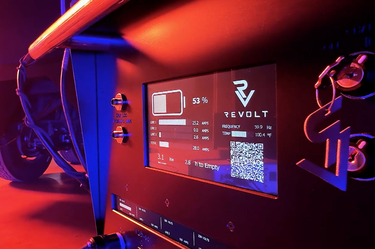
革新高壓移動供電的電氣化之路
ReVolt 為電影片場注入活力!了解他們如何使用 Vicor 高密度電源模組取代柴油,實現清潔的移動供能
電源架構為何制約新太空 AI 任務
衛星 AI 的發展速度已經超越了傳統電源系統。 現代計算需要超低電壓、大電流的供電能力,而傳統電源架構直到現在都無法滿足這一需求
AI 在太空賦能快速通訊,開啟創新新紀元
Spacechips 攜手 Vicor 打造了 AI1 應答器,這是現時在軌運行中功率密度最高的處理器板。 分比式電源架構可提供 133 TOPS 算力用於實时衛星自主運行和 130A 處理