Optimizing DC-DC converter stability: AC and transient analysis in simulations of source impedance effects
Learn how to optimize DC-DC converter stability through AC analysis in the frequency-domain and transient analysis in the time-domain
Tutorial by Jonathan Siegers, Principal Applications Engineer and Vamshi Domudala, Application Engineer
The previous tutorial in this series highlighted the performance, flexibility, and speed benefits of using power modules to design power systems, then provided an overview of the modular design process. A modular design strategy is powerful, but it requires support circuitry in the power delivery network (PDN) to form a complete power system. This second part of the tutorial series addresses the first PDN issue: filtering electrical noise on the input and output sides of a switching DC-DC module.
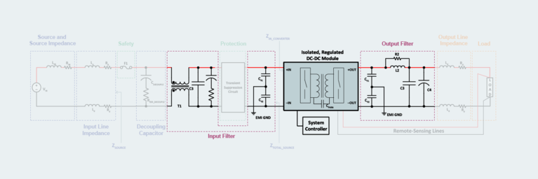
Complete power system filtering elements required to mitigate switching converter noise.
The switching action of DC-DC converters and parasitic circuit elements distributed throughout the PDN cause two types of noise currents that must be filtered: common-mode and differential-mode.
Common-mode noise originates from the high-voltage switching nodes present inside the converter coupled through parasitic capacitance to an EMI ground reference. This noise travels in-phase out of the converter’s positive and negative input terminals and closes through the system’s ground reference. The converters’ switching action also generates differential-mode noise, but its travel is limited to the circulation between the input terminals of the converter.
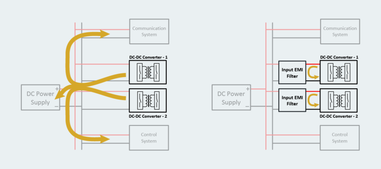
If left unchecked, this noise can cause a host of problems within the power system. The following figure shows two DC-DC converters that share a point of common coupling with a DC source, as well as control and communication systems, which are typically sensitive to noise. DC-DC converter-generated noise circulating throughout the PDN can cause erratic system operation and negatively influence the overall behavior of adjacent systems that share an electrical connection.
Noise from the converter propagates out of the module and can cause significant problems for control and communication systems.
Input filters added to the system bypass switching converter noise locally so that the noise circulates only between the filter and the DC-DC converter itself, reducing interference with other systems connected to the same source. The filter also works in the opposite direction, decreasing the DC-DC converters’ susceptibility to noise that comes from external sources.
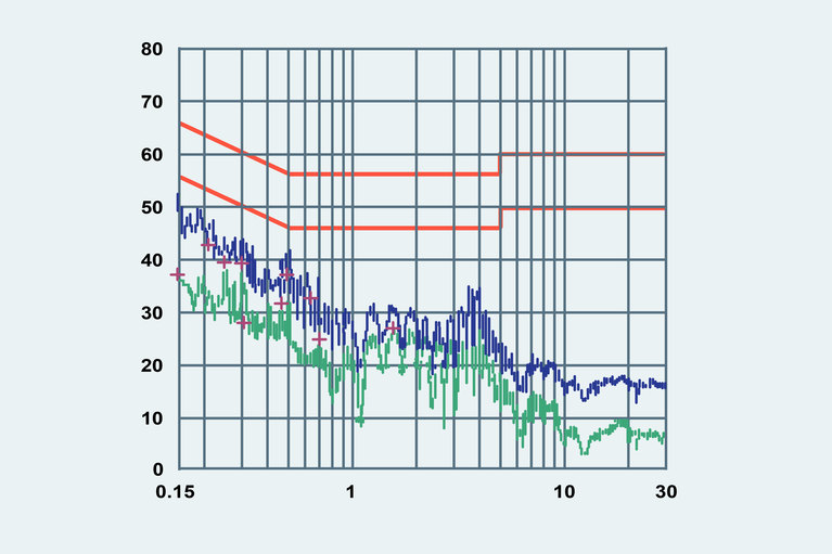
To begin designing a filter into the system, first note that the filtering for a given application may have to meet specific electromagnetic compatibility standards set forth by various international bodies for both electromagnetic compatibility (EMC) and EMI. Standards can vary significantly by industry and application; defense application compliance is significantly different from automotive, for example.
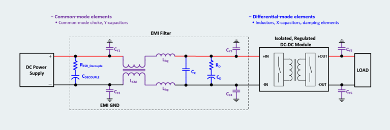
Noise-mitigation techniques require several discrete components to filter both common-mode and differential-mode noise currents effectively. Common-mode filtering is generally achieved with a common-mode choke, which forms a high-impedance series path for common-mode currents that flow out of the converter along with both the positive and negative input terminals. The common-mode choke works alongside Y-capacitors that form a shunt path for the common-mode noise to the EMI ground shown in the figure below.
Discrete components of the system that filter common-mode and differential-mode noise.
Differential-mode elements include X-capacitors and series differential inductors to perform similar functions. This ensures that there is a high-impedance series path for differential-mode noise from the converter, and a low-impedance shunt path for the noise current to close locally to the converter.
When routing noise currents to ground, it is possible to couple noise from the power components into the control components by connecting the signal and power grounds incorrectly. When coupled by trace parasitics into signal components, the high-frequency noise propagated by the DC-DC converter can impact low-power control signals and, in turn, cause erratic operation. To prevent power current from flowing through signal grounds, connect the signal ground and the power ground at a single point only.
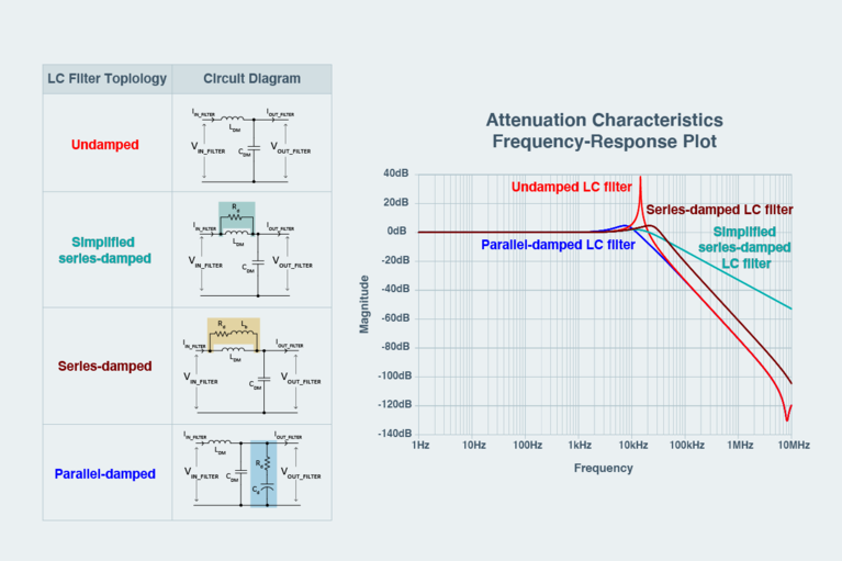
While there are several different methods for constructing filter topologies, this tutorial will illustrate only the more common second-order responses for filters, the first of which is a simple inductor and capacitor. The following figure shows an undamped LC filter response with a second-order roll-off at –40dB per decade above the cut-off frequency. Undamped LC filters are generally not suitable solutions due to their characteristic resonance at the corner frequency. Without proper damping, this filter topology will amplify noise in the range of frequencies around the resonance. There are several damping strategies to consider—first, a simplified series-damped filter circuit with a resistor in parallel with the inductor. The damping at the corner frequency is much better, but it comes at the cost of decreased high-frequency attenuation due to the addition of a zero in the filter’s frequency response.
Three damping approaches compared to an undamped LC filter in a system that exhibits second-order roll-off at –40dB.
A second, better approach adds an inductor that selectively applies damping resistance into the circuit, maintaining the second-order filter response with improved damping around the resonant frequency. However, this approach shifts the corner frequency slightly. A third alternative is adding a parallel R-C damping branch, which significantly improves damping around the corner frequency of the filter.
To design an output filter, first define the output voltage ripple magnitude that the application can tolerate. Next, consider the dynamics of the load current, including high di/dt load transients. Of the several pieces of a DC-DC system design that handle high dynamic loads, the converter’s output filter supplying that load has the most direct impact because of its series inductance. With the maximum di/dt of the load defined, it is possible to set a constraint on the inductor’s maximum value for use in the system. The following equation to determine the inductor value factors in the di/dt of the load and the maximum voltage drop allowed across that inductor during a transient, i.e., the low-line input operating voltage at the load.

Next, after selecting the appropriate inductor, determine the cut-off frequency for the filter based on the ripple and how much attenuation is needed at the output. From this information, it is then possible to work out the capacitance value using this equation:

DC-DC switching converters today operate at very high frequencies — high enough that parasitic capacitances and inductances in the design layout can significantly impact the filter’s overall behavior in the converter system.
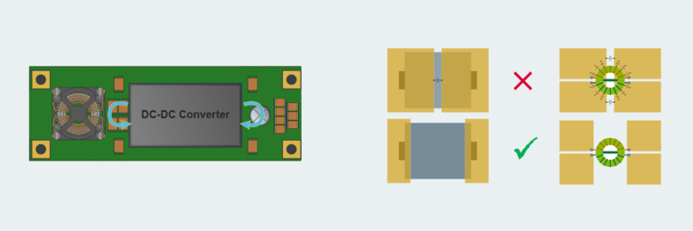
In general, EMI filters should be located physically close to the converter itself. The following figure shows a DC-DC converter with filtering capacitances placed directly at the input. Due to the proximity to the converter, the noise currents circulate locally. If the noise currents were allowed to circulate in a wider space, the loop path could very easily become an antenna at high frequency, radiating noise to other parts of the circuit and completely negating the benefit of adding a filter. Therefore, both the series and shunt filter elements should be placed as close as possible to the DC-DC converter to limit the size of the loop that will experience high frequency and high di/dt currents.
PCB layout considerations include placing filter components in close proximity to the DC-DC converter (left). Separating copper planes to avoid capacitive coupling allows noise currents to bypass the high-impedance filter components (right).
The layout of the PCB is also important. Pay careful attention to the traces that will be carrying noise currents to minimize their overall inductance and resistance so that at high frequency they will not form significant voltage as a result of their impedance.
Also, lay out planes on the PCB to avoid forming parasitic capacitances that allow coupling effects to bypass the filtering elements. For example, if the copper planes that define the connection to a filter inductor’s terminals are too close together, a parasitic capacitance will allow high-frequency currents to bypass the high-impedance inductor. Best practices separate the copper planes to minimize parasitic capacitance around high-series-impedance components.
The same concept applies to common-mode chokes. Maintain a keep-out area around the common-mode choke windings to prevent parasitic capacitance that would bypass the filter component.
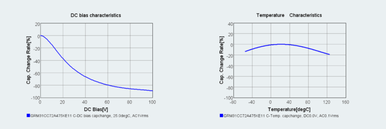
Filtering-component performance can vary significantly under fluctuating environmental or application related conditions. For example, the effective value of Class 2 dielectric ceramic capacitor exhibits significant variation with applied DC bias voltage. The DC bias characteristic chart below illustrates this effect on an example 1206 size MLCC component; at 50V applied bias, the effective capacitance is reduced by 74%. This variation in effective capacitance will increase the filter’s corner frequency, reducing the attenuation achieved at high frequencies.
DC bias characteristics (left) and Temperature characteristics (right): The effects of voltage and temperature on effective capacitance are important considerations for filter design. DC bias characteristics significantly change the capacitance of a Murata Class 2 dielectric ceramic capacitor (left), and significant reductions in capacitance are evident at the extremes of the rated temperature range (right). Source: Murata Manufacturing Co., Ltd.
Operating temperature can also have a significant impact on effective capacitance. The temperature characteristics chart above shows that the same example capacitor exhibits up to a 20% reduction in effective capacitance when operated to the extremes of its rated operating temperature range. A robust filtering solution for DC-DC modules must account for the impact of expected component variation over the system’s full expected operating range.
Integrating the input filter into the system poses additional challenges for overall system stability. The next tutorial in this series will take up that area of system design.
Also in this series:
How to design modular DC‑DC systems, part 1: four stages of design
How to design modular DC‑DC systems, part 3: stability analysis and decoupling
How to design modular DC‑DC systems, part 4: safety protection systems
How to design modular DC‑DC systems, part 5: load considerations
Innovation: 48V direct to low voltage conversion
Webinar rebroadcast: EMI challenges and troubleshooting techniques
White paper: Practical EMI control in a power component design space
Optimizing DC-DC converter stability: AC and transient analysis in simulations of source impedance effects
Learn how to optimize DC-DC converter stability through AC analysis in the frequency-domain and transient analysis in the time-domain
Power modules simplify creepage and clearance design solutions for electric vehicles
Overmolding is the key to solving arcing issues in 48V automotive power systems
Current multipliers: The obvious choice for powering AI processors and other demanding applications
AI processors need to handle low-voltage, high-current demand, which can cause power system bottlenecks. Learn how current multiplication can change that.
High-performance ZVS buck regulator removes barriers to increased power throughput in wide‑input-range point-of-load applications
Today's higher performance applications require more than what conventional regulators can offer. Learn how ZVS topology can boost your performance.

