15 technical challenges to consider and conquer when designing a 48V power delivery network
To help better prepare for your 48V migration, consider the following 15 challenges as you embark on your first 48V designs
Buck voltage regulation, an essential part of distributing power from a DC supply to its points of load (PoLs), has typically been implemented with a PWM circuit. The PWM duty cycle is varied to accommodate the required voltage reduction.
However a couple of factors have applied increasing pressure to regulator design. Firstly, power density is being forced up as continuously more powerful devices are designed onto boards without corresponding increase in footprint. Secondly, DC power supply voltage levels are tending to rise to minimize distribution losses, while device voltages are reducing to increase internal speed and efficiency. These trends combine to increase the voltage drop and associated switching losses across the regulator.
For example a process control system may call for regulation from 24V to 3.3V – a gap that would typically be covered using two regulation stages; increasing board space, cost and reliability issues. The regulator’s switching frequency is also limited, as increased switching activity incurs more losses. This in turn limits the use of smaller passive components for filtering, penalizing the density of the total solution.
Although high-density PWM regulators have evolved with improved IC integration, MOSFETs and packaging, their design is no longer sufficient to meet the power demands they face. This is mainly due to switching losses within the regulator MOSFETs. These must be overcome or avoided to achieve any significant boost to regulator performance.
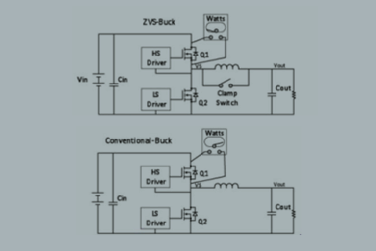
A better solution uses zero-voltage-switching (ZVS) topology, which allows for operation at a higher frequency and at higher input voltages without sacrificing efficiency. While still PWM based, a separate phase is added to the PWM timing to allow for ZVS operation. Figure 1 compares a conventional buck regulator with a version modified for ZVS operation. Utilizing the added phase, the ZVS type uses the clamp switch and circuit resonance to operate the high side (Q1) and synchronous (Q2) MOSFETs efficiently with soft switching, avoiding the losses they incur during conventional PWM operation and timing.
For example in the conventional circuit, as Q1 is turned on and Q2 turned off, a very high current flows through the MOSFET pair, since Q2’s body diode appears as a short circuit during its reverse recovery time. Other losses arise due to discharging Q1’s output capacitance, and to reverse recovery in Q2. These losses increase as the switching frequency or input voltage increases.
By contrast the ZVS design addresses the high turn-on losses of the conventional regulator by eliminating high current body diode conduction prior to turn on of the high-side MOSFET, bringing the D-S voltage of the high side MOSFET to zero or nearly zero and producing no high current spikes or damaging ringing. The ZVS action applied to Q1 removes its Miller effect at turn on, allowing the use of a smaller driver and lower gate drive.
Vicor has utilized ZVS topology within our buck regulators. These provide regulation up to 36VIN at a higher efficiency and from a smaller form factor than achievable from conventional hard switching, high density regulators.
Figure 1: ZVS Buck
Related content
Product overview: buck regulators
15 technical challenges to consider and conquer when designing a 48V power delivery network
To help better prepare for your 48V migration, consider the following 15 challenges as you embark on your first 48V designs
Future-proof automotive high-voltage-to-SELV conversion
Legacy 12V architecture is no longer capable of sustaining the rising electronic loads in automobiles. Learn how power modules hasten the transition to 48V
Power modules simplify creepage and clearance design solutions for electric vehicles
Overmolding is the key to solving arcing issues in 48V automotive power systems
Power under pressure: Meeting the military’s surging energy demands
More capability (power) and compatibility are in demand for military power system designers. Learn how the Vicor SOSA Power Supply solves this problem


